RDM Innovation: Mastering Multi-Layer PCB Design
FAQs on Multi-Layer PCB Design
-
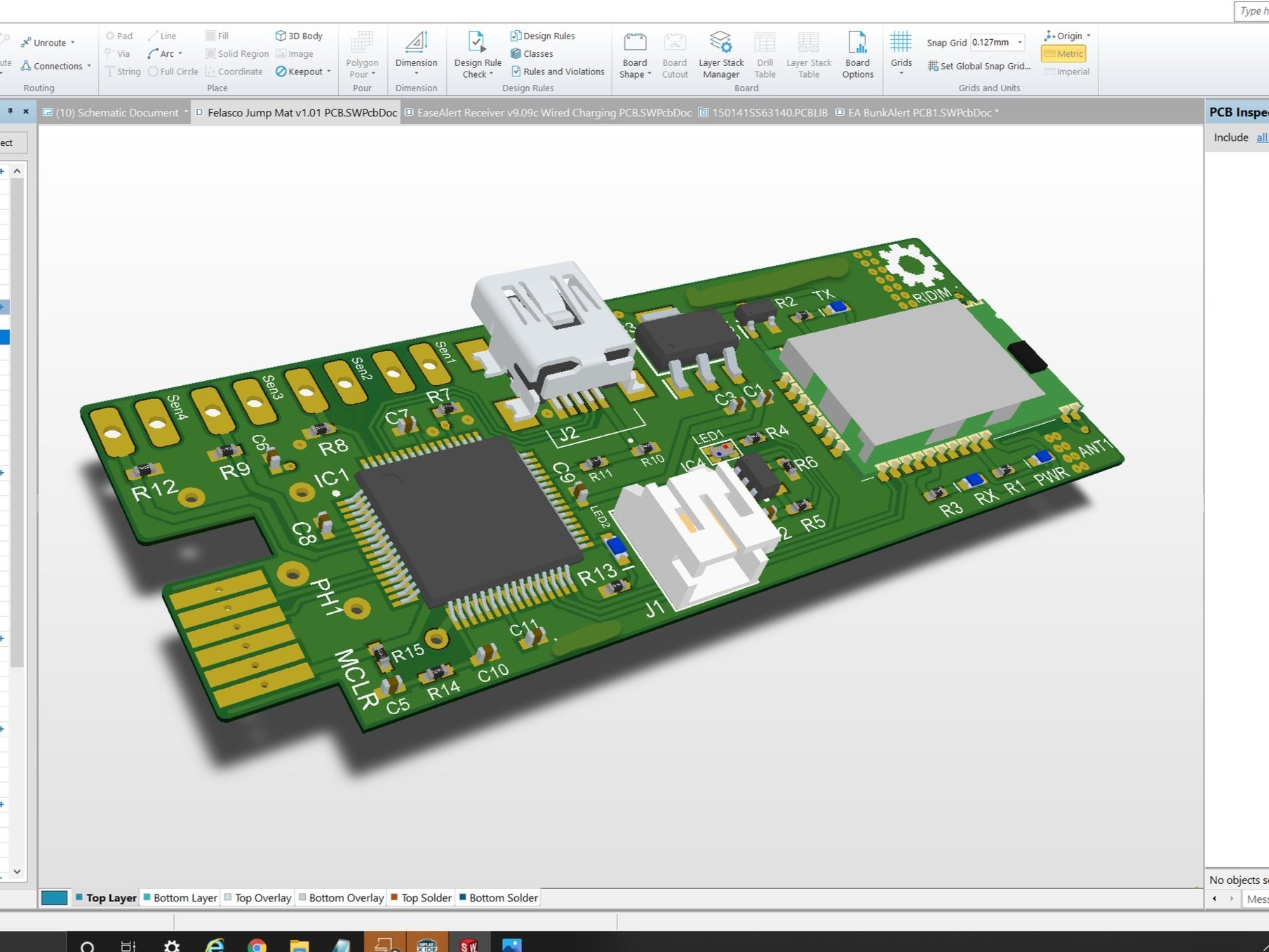
At RDM Innovation, our approach is methodical and technology-driven. We begin with a detailed requirement analysis, followed by schematic design and layout planning with tools like Altium Designer or Cadence Allegro. We focus on stack-up design, ensuring optimal signal path length, impedance control, and layer-to-layer transitions. Our engineers employ advanced simulation tools to predict performance, addressing issues like crosstalk, signal integrity, and thermal dissipation before physical prototyping. We also consider manufacturing constraints early in the design phase to ensure designs are not only innovative but also producible.
-
Our PCBs stand out due to our focus on engineering excellence and customization. We don't just design; we engineer solutions with performance in mind. Our use of high-quality materials, meticulous layer planning for power and ground planes, and stringent design rules for high-speed signals set us apart. Additionally, our commitment to DFx (Design for Manufacturing, Assembly, Test, etc.) principles ensures that our designs are not just theoretical but ready for real-world application. Our iterative design process, backed by thorough testing and simulation, results in PCBs that meet or exceed performance expectations.
-
We have extensive experience designing PCBs with up to 20+ layers. Each additional layer offers advantages in routing complex signals, managing power distribution, and enhancing thermal performance. For instance, in high-end server applications or sophisticated medical equipment, we've used 16 to 24 layers to manage high-speed data paths, multiple voltage rails, and advanced shielding techniques. Our approach scales with complexity, ensuring that even the most demanding designs are executed with precision.
-
Material selection is a critical aspect of PCB design. We consider the operational environment, electrical performance requirements, and mechanical constraints. Standard FR-4 is often used for cost-effective solutions, but for high-frequency applications, we might opt for materials like Rogers or PTFE-based substrates for lower dielectric loss. For thermal management, we might incorporate metal core PCBs or high-Tg materials to handle higher temperatures. Each choice is made with an eye toward matching the material's properties with the project's specific demands, such as signal speed, layer count, and environmental resilience.
-
Quality assurance starts with design. We implement DFM checks, use automated design rule checks (DRC), and run simulations for thermal and electrical performance. Prototyping is followed by comprehensive testing, including electrical testing, thermal imaging, and environmental stress testing. We use IPC standards as a baseline but often exceed them to ensure reliability. Our process involves peer reviews at critical design stages, and we maintain a feedback loop from manufacturing to design to refine our techniques continually.
-
We start with a thorough design review followed by a small-scale prototype build, where we validate the design's functionality and manufacturability. We use this phase to tweak designs if necessary, focusing on yield improvement. Once prototypes pass our rigorous testing, we move to small-batch production to ensure scalability. Here, we monitor yield rates, quality metrics, and cost implications. Full-scale production only commences when we're confident in the design's performance, manufacturability, and cost-effectiveness. Throughout, we keep a close eye on supply chain logistics to ensure timely delivery.
-
Customization begins with a deep dive into your application's requirements. Whether it's optimizing for signal integrity in high-speed data systems, ensuring compliance with stringent medical standards, or designing for harsh automotive environments, we tailor our design approach. This might involve custom stack-ups, specialized EMI shielding techniques, or integrating unique components. We collaborate closely with clients, often involving their engineers in the design process, to ensure the PCB not only meets but enhances the product's performance metrics.
-
Starting a project with us is straightforward. Contact us via our website's form or directly at contact@rdminnovation.com. We'll arrange a technical consultation where we'll discuss your project's specifications, timelines, and any unique challenges. From there, we'll draft a project scope, propose initial design concepts, and outline the development roadmap. Our aim is to create a partnership where your engineering insights combine with our PCB design expertise to deliver exceptional results.

